
R&D LAB 4.4 «COMPUTER-AIDED DESIGN OF MICRO- AND NANOELECTRONIC SYSTEMS»
|
|
|
|
FIELD OF EXPERTISE
- Theoretical studies, computer simulation and design of manufacturing processes of semiconductor devices, integrated sensors and integrated circuits (IC) components, including of the types that are operating under destructive conditions such as extremely high temperatures, ionising radiation, etc.
- Research and simulation of novel materials and structures characteristics, including nano-sized and biological objects, based on methods of molecular dynamics and quantum mechanics (as the fundamental principles), and with the use of cluster hardware (supercomputers)
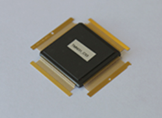
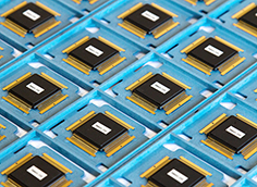
- Custom design of analog, digital and mixed IC; preparation of projects for manufacturing on the base and with the use of submicron technological processes of the world's leading foundry-manufacturers
- Development of mathematical methods and algorithms, as well as of special-purpose software, targeted at statistic analysis and optimization of the process and device structures parameters in the end-to-end IC design cycle, at manufacturing processes, extraction and verification of the SPICE-model parameters of semiconductor devices, and etc.
SERVICES
- Joint fundamental and applied research as well as joint educational projects with foreign research and educational institutions
- Training of highly-qualified professionals coming from neighbouring and other countries (Master, PhD & postgraduate training)
- Implementation of fundamental and applied research results and developments into the educational process
2020 – 2023 PROJECTS
Scientific and technical projects are carried out within the framework of international and national programs, including jointly with partners.
1. Absorption of terahertz radiation by quasi-two-dimensional magnetic materials based on MAX3 chalcogenides of transition metals for nanoplasmonic devices.
2. Structural, electronic and magnetic properties of yttrium-aluminum and yttrium-iron garnets and perovskites doped with neodymium.
3. Methods for designing and optimizing constructive solutions for semiconductor microstrip detectors and sensor systems based on them.
4. Absorption properties of materials in Van Der Waals heterostructures used as structural elements in transparent and flexible electronics.
5. Development of design and optimization methods for programmable logic integrated circuits based on static random access memory.
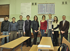
MANAGMENT
Ivan Lovshenko
Head of the laboratory
☏ +375 17 293 88 90
🖂 lovshenko@bsuir.by
View profile
Viktor Stempitsky
PhD, Associate Professor
☏ +375 17 293 84 24
🖂 vstem@bsuir.by
View profile
CONTACTS
6, P. Brovki str., 220013, Minsk, Republic of Belarus
☏ +375 17 293 84 09
🖷 +375 17 390 96 28
🖂 lovshenko@bsuir.by
✎ Office 119