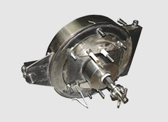
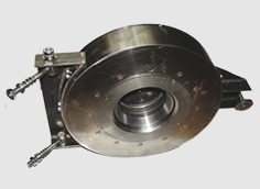
DOUBLE-BEAM ION SOURCE BASED ON ACCELERATOR WITH ANODIC LAYER DBIS-001
|
|
|
|
PURPOSE
Double-beam ion source based on accelerator with anodic layer DBIS-001 is designed for deposition of thin films of metals, semiconductors and dielectrics by ion-beam and reactive ion-beam sputtering. DBIS is also applied for ion cleaning of substrate surfaces and for surface activation. It has two separate stages for ion beam generation, so that two independent ion beams are created, one of which is used for sputtering of the target material, and the other one – for ion pre-cleaning of substrates and for ion assistance.
APPLICATION AREA
- ion-beam sputtering
- reactive ion-beam sputtering
- double beam ion sputtering
- ion-beam assisted deposition (IBAD) with electron-beam, laser and arc evaporators
- ion-beam assisted magnetron (IBAM)
- ion pre-cleaning of surface
- formation of substrate film transition layer (ion mixing)
- ion etching with the ability to use reactive gas
TECHNICAL CHARACTERISTICS
Sputtering stage
| Target diameter, mm | 80 |
| Anode voltage (DC), V | 800...6000 |
| Ion energy, eV | 300...2000 |
| Discharge current, mА | up to 300 |
| Ion beam current, mА | up to 250 |
| Working pressure, Pа | 0,01...0,06 |
| Gas flow, scc/min | up to 40 |
| Working gases | Ar, O2 , N2 , CH4 , etc. |
| Deposition rate, nm/sec | up to 0,8 |
Assisting stage
| Anode voltage (DC), V | 400...3000 |
| Ion energy, eV | 300...1000 |
| Ion beam current, mА | up to 120 |
| Working pressure, Pа | 0,01...0,06 |
| Working gases | Ar, O2 , N2 , CH4, etc. |
| Size, mm | Ø 318х255 |
| Weight, кg, not more | 15 |
ADVANTAGES
- an electromagnet is used as a source of the magnetic field, thus allowing an optimization of the magnetic field induction in the acceleration channel, and an increase in the ion beam generation efficiency
- the ion source is used for sputtering of metallic, semiconductor and dielectric (SiO2, BN, graphite, etc.) targets
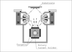
- the ion source may be equipped with a rotary target holder with four targets of different material to form multilayer structures within a single vacuum cycle
- supplementary equipping the ion source with a rotary target holder permits to sputter mosaic targets to obtain multi-component layers
- it is possible to obtain component films by applying mixtures of rare and reactive gases (oxygen, nitrogen, etc.) at sputtering of metallic targets
DEVELOPER
Center 2.1 "Plasma Processing Research Center"
CONTACTS
6, P. Brovki str., 220013, Minsk, Republic of Belarus
☏ +375 17 293 80 79, +375 17 293 88 35
🖷 +375 17 293 88 35
🖂 svad@bsuir.by ; szavad@bsuir.by
🌐 plasma.bsuir.by
OTHER INNOVATIONS IN THIS AREA
PLASMA ELECTRON SOURCE FOR ION BEAM NEUTRALIZATION


