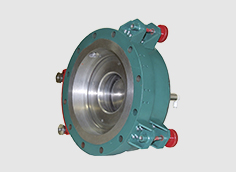
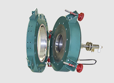
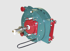
SPUTTERING ION SOURCE BASED ON ACCELERATOR WITH ANODIC LAYER SPIS-002
|
|
|
|
PURPOSE
The sputtering ion source SPIS-002 based on the accelerator with anodic layer is intended for deposition of thin films of metals, semiconductors and dielectrics by ion-beam and reactive ion-beam sputtering methods.
APPLICATION AREA
- ion-beam sputtering
- reactive ion-beam sputtering
TECHNICAL CHARACTERISTICS
| Target diameter, mm | 80 |
| Anodic voltage (DC), V | 800...6000 |
| Ion energy, eV | 300...2000 |
| Discharge current, mA | up to 300 |
| Ion beam current, mA | up to 250 |
| Working pressure, Pa | 0,01...0,06 |
| Gas flow, m/sec | up to 40 |
| Work gases | Ar, O2 , N2 , CH4 и т.д. |
| Deposition rate (Al), nm/sec | up to 0,8 |
| Size, mm | Ø 307х296 |
| Weight, kg, not more | 12 |
ADVANTAGES
- the ion source allows sputtering of metallic, semiconductor and dielectric (SiO2, BN, graphite, etc.) targets
- an electromagnet is used as a source of the magnetic field, thus allowing an optimization of the magnetic field induction in the acceleration channel, and an increase in the ion beam generation efficiency
- a unique construction of the flange mounting and removable target unit of the ion source provides an easy access for an operator to change targets and clean the ion sources
- ion source may be equipped with a rotary target holder for four targets of different material to form multilayer structures within a single vacuum cycle
- a possibility to turn the sputtering ion source into an assisting one by replacing the parts of the discharge area and mounting the target unit
- it is possible to obtain component films by applying mixtures of rare and reactive gases (oxygen, nitrogen, etc.) at sputtering of metallic targets
DEVELOPER
Center 2.1 "Plasma Processing Research Center"
CONTACTS
6, P. Brovki str., 220013, Minsk, Republic of Belarus
☏ +375 17 293 80 79, +375 17 293 88 35
🖷 +375 17 293 88 35
🖂 svad@bsuir.by ; szavad@bsuir.by
🌐 plasma.bsuir.by
OTHER INNOVATIONS IN THIS AREA
PLASMA ELECTRON SOURCE FOR ION BEAM NEUTRALIZATION


