
ION BEAM ASSISTED SOURCE BASED ON ACCELERATOR WITH ANODIC LAYER ASIS-002
|
|
|
|
PURPOSE
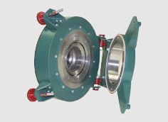
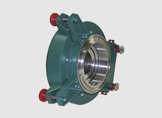
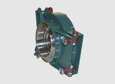
Ion beam assisted source based on accelerator with anodic layer ASIS-002 is designed for pre-cleaning of substrates, as well as for ion-beam etching, ion-beam assisted deposition of thin films and direct beam deposition.
APPLICATION AREA
- ion-beam assisted deposition (IBAD) in combination with electron-beam, laser, arc evaporators or ion-beam sputtering systems
- formation of substrate film transition layer (ion mixing)
- ion pre-cleaning
- ion-beam etching with the ability to use reactive gas
- direct beam deposition (DiBD)
- ion-beam assisted magnetron sputtering (IBAM)
TECHNICAL CHARACTERISTICS
| Anode voltage (DC), V | 450...6000 |
| Ion energy, eV | 150...2000 |
| Ion beam current, mА | up to 200 |
| Working pressure, Pа | 0,01...0,06 |
| Gas flow, scc/min | up to 40 |
| Working gases | Ar, O2, N2, hydrocarbons, etc. |
| Size, mm | Ø 298х175 |
| Weight, кg, not more | 9 |
ADVANTAGES
- an electromagnet is used as a source of the magnetic field, thus allowing an optimization of the magnetic field induction in the acceleration channel, and an increase in the ion beam generation efficiency
- it is possible to change the inclination angle of the ion beam by replacing the parts in the discharge area of the ion source
- it is possible to turn the sputtering ion source into an assisting one by replacing the parts of the discharge area and to install the target unit
- the RF/DC magnetron can be included into the structure of the ion source. This permits to implement the method of the ion beam assisted magnetron sputtering (IBAM)
- the ion source may be supplementary equipped with a filament-free ion beam neutralizer
- a unique construction of the flange mounting of the ion source provides an easy access for an operator to clean the ion source
- the use of the ion assistance makes it possible to increase the adhesion of the deposited layers, reduce the porosity of the deposited layers, control internal stress in a layer, and stoichiometry when depositing the compounds
DEVELOPER
Center 2.1 "Plasma Processing Research Center"
CONTACTS
6, P. Brovki str., 220013, Minsk, Republic of Belarus
☏ +375 17 293 80 79, +375 17 293 88 35
🖷 +375 17 293 88 35
🖂 svad@bsuir.by ; szavad@bsuir.by
🌐 plasma.bsuir.by
OTHER INNOVATIONS IN THIS AREA
PLASMA ELECTRON SOURCE FOR ION BEAM NEUTRALIZATION